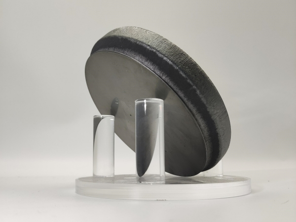
1. Technical Overview
Single-crystal diamond substrate wafers feature grain-boundary-free structure, ultra-low defect density, superior thermal conductivity uniformity, excellent optical homogeneity, and reliable insulation stability. Owing to these comprehensive advantages, they have become core substrate materials for high-end RF power devices, quantum optical devices, high-precision optical windows, and superconducting detection devices. Compared with conventional polycrystalline diamond substrates, single-crystal diamond eliminates grain boundary scattering, thermal resistance fluctuation, and optical anisotropy, fully satisfying the ultra-high precision, stability, and reliability requirements of advanced electronic and photonic devices.
Among diverse diamond fabrication technologies, Bias-Enhanced Nucleation (BEN) is the only mature CVD core technique that enables
in-situ orientation-controllable nucleation in the industry. Different from external seeding methods such as electrostatic seeding and mechanical seeding, BEN technology generates uniformly oriented diamond nuclei inside the CVD chamber through electric field modulation without introducing exogenous nano-diamond particles. It fundamentally improves the crystalline quality, orientation consistency, and defect performance of
single-crystal diamond substrates, serving as an indispensable core process for heteroepitaxial growth of large-size and high-quality single-crystal diamond wafers.
2. Core Technical Challenges of Single-Crystal Diamond Epitaxy
The fabrication of high-end single-crystal diamond substrates imposes extreme requirements on nucleation quality, including not only high-density nucleation sites but also highly unified grain orientation, ultra-low defect density, and complete elimination of random grain boundaries. Traditional pretreatment processes have inherent technical bottlenecks. Electrostatic seeding and mechanical seeding rely on the adsorption of external diamond particles with random and disordered orientations. The grown films exhibit strong grain anisotropy, numerous grain boundaries, and high defect density, which can only form polycrystalline structures and fail to meet single-crystal epitaxy standards.
Furthermore, conventional heteroepitaxy suffers from severe lattice mismatch and significant surface energy difference between the substrate and diamond, easily causing random nucleation, chaotic orientation, and interfacial defect accumulation. These problems lead to low single-crystal yield, limited wafer size, and poor performance consistency. As a targeted solution, electric-field-assisted in-situ controllable nucleation via BEN thoroughly solves the orientation uncontrollability and high defect defects of traditional processes, becoming the core approach for preparing large-size single-crystal diamond substrates on iridium and other conductive substrates.
3. Core Principle and Standardized Process Flow of BEN Technology
BEN (Bias-Enhanced Nucleation) is a critical pretreatment procedure prior to diamond epitaxial growth. It adopts a synergistic mechanism of
electric-field accelerated ion bombardment and selective etching to realize in-situ, controllable, and orientation-unified diamond nucleation. The entire process is highly standardized with precise parameter controllability, perfectly matching the mass production requirements of high-precision single-crystal diamond substrates.
The complete BEN process consists of two core stages:
Stage 1: Bias-enhanced nucleation pretreatment. The gas atmosphere of the CVD chamber is adjusted to a high-carbon environment with a maximum CH₄/H₂ ratio of 40%. A constant negative DC bias is applied to the conductive substrate. The strong electric field accelerates carbon and hydrogen plasma ions to bombard the substrate surface at high speed, driving carbon ions to implant into the near-surface region and forming high-density, orderly arranged sp³ diamond nucleation sites.
Stage 2: Conventional epitaxial growth. After uniform nucleation is completed on the substrate surface, the external bias is removed. The chamber is switched to low-methane conventional growth parameters to reduce the growth rate and optimize crystalline quality. The oriented nuclei grow vertically and merge horizontally, eventually forming low-defect and high-consistency single-crystal diamond substrate wafers.

【Figure 1】Schematic diagram of the original Yugo microwave CVD-BEN experimental setup

【Figure 2】High-resolution SEM morphology comparison of substrate surfaces under two sets of different BEN process parameters

【Figure 3】Schematic diagram of dual-bias assisted hot-filament CVD BEN reactor
4. Process Compatibility and Threshold Characteristic Parameters
BEN technology possesses excellent equipment compatibility, applicable to two mainstream industrial systems: microwave CVD and dual-bias modified hot-filament CVD. The nucleation density and grain orientation can be precisely regulated through multi-dimensional parameter optimization. The process features a strict voltage threshold with a narrow and controllable parameter window, which is critical for guaranteeing single-crystal crystalline quality.
Core process characteristics: When the substrate negative bias is higher than -70 V, the ion bombardment energy is insufficient to trigger effective diamond nucleation. The optimal bias range is -100 V, which delivers high nucleation density, superior orientation consistency, and minimal defects. Under standard conditions, the BEN nucleation density can be stably maintained at an ultra-high level of 10¹⁰ ~ 10¹³ cm⁻², which can be flexibly adjusted according to substrate size and thickness requirements, fully adapting to the preparation of large-size single-crystal diamond wafers.
5. Two Classical Industrial BEN Nucleation Mechanism Models
After years of technological iteration and academic verification, two authoritative classical mechanism models have been widely recognized by academia and industry, systematically explaining the microcosmic formation principle of high-quality single-crystal diamond via BEN technology:
5.1 Ion Bombardment and Selective Etching Model
High-energy carbon ions accelerated by the electric field implant into the substrate surface layer to form a hybrid carbon-substrate transition layer. Meanwhile, hydrogen radicals in the plasma exhibit strong selective etching performance, which preferentially removes disordered sp² non-diamond carbon structures and retains structurally stable and orientation-unified sp³ diamond nuclei. The remaining nuclei grow continuously with preferential orientation, ultimately forming highly ordered single-crystal diamond structures.
5.2 IBI-BLG Ion Bombardment Induced Lateral Growth Model
This model is mainly applied to the preparation of large-size single-crystal diamond on iridium substrates. Under negative bias, a thin amorphous hydrogenated carbon (a-C:H) layer is formed on the substrate surface. High-energy ion bombardment induces lateral expansion and orientation regularization of buried diamond domains. After nucleation, the disordered defective carbon layer on the surface is stripped by hydrogen plasma etching, leaving only highly oriented diamond domains at the interface. Subsequent epitaxial growth directly forms large-area, grain-boundary-free, and low-defect single-crystal diamond substrate wafers.

【Figure 4】Schematic diagram of Yugo BEN ion bombardment nucleation mechanism

【Figure 5】Physical image of 92 mm large-size single-crystal diamond wafer fabricated via BEN process
6. Core Advantages and Application Boundaries of BEN Process
6.1 Core Technical Advantages
Compared with traditional nucleation technologies, BEN exhibits exclusive superiority in single-crystal quality. The entire in-situ nucleation process requires no exogenous particle introduction, completely avoiding impurity contamination. The highly unified grain orientation eliminates intrinsic grain boundary defects of polycrystalline diamond. The fabricated single-crystal
diamond substrates present excellent uniformity in thermal conductivity, optical transmittance, and electrical insulation performance, fully complying with the stringent standards of high-end RF, quantum, superconducting, and precision optical devices. It is an irreplaceable core process for mass production of high-grade single-crystal diamond.
6.2 Process Limitations and Application Boundaries
BEN technology has clear application restrictions. Relying on electric-field ion bombardment, it is only applicable to conductive substrates, with iridium substrates achieving the best compatibility. It cannot be directly used for single-crystal growth on insulating substrates such as sapphire and AlN, requiring complementary cooperation with electrostatic seeding and other processes. In addition, BEN features a narrow parameter window, high equipment precision requirements, and complex process debugging, resulting in a much higher mass-production threshold than conventional polycrystalline seeding processes.
7. Summary of Core Process Parameters
The parameter accuracy of BEN directly determines the crystalline quality and performance consistency of single-crystal diamond substrates. The core process parameters are summarized below for scientific research reference and mass production parameter calibration:
| Parameter / Performance Dimension |
Core Specification / Characteristics |
| Effective nucleation bias threshold |
≤ -70 V, optimal range: -100 V |
| Chamber methane concentration |
Maximum 40% CH₄/H₂ ratio (conventional) |
| Nucleation density range |
10¹⁰ ~ 10¹³ cm⁻² |
| Applicable equipment systems |
Microwave CVD, dual-bias modified hot-filament CVD |
| Applicable substrate type |
Conductive substrates only (iridium substrate optimal) |
| Main products |
Low-defect, high-orientation single-crystal diamond substrates |
8. Comprehensive Process Summary
In the field of high-end single-crystal diamond substrate mass production, BEN bias-enhanced nucleation technology is irreplaceable. It fundamentally solves the industry pain points of traditional processes, including low single-crystal yield, limited wafer size, high defect density, and poor performance consistency. Benefiting from its in-situ controllable nucleation, unified grain orientation, low defect density, and contamination-free characteristics, BEN has become the core supporting technology for heteroepitaxial fabrication of large-size and high-quality single-crystal diamond substrates.
JXT specializes in high-performance diamond substrate materials. We stably supply high-purity single-crystal diamond substrates, high-performance
polycrystalline diamond substrates, and customized diamond films, fully meeting the differentiated demands of high-end scientific research, precision device R&D, and industrial mass production.